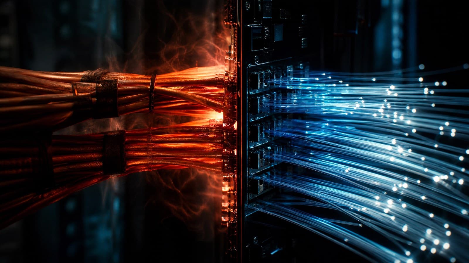
The problem starts in physics, not technology
For fifty years the chip industry did one thing well: pack more transistors into the same area.
And through all those years, the wire connecting the chips stayed copper.
That has now broken. A modern AI accelerator can process data faster than the electrical connection can feed it. The bottleneck moved from compute to transport - not because nobody tried to improve copper, but because it hit a physical limit.
Copper's three limits
a. Heat
Copper resists current. Resistance produces heat. Heat requires cooling. Cooling requires power.
And that is a self-feeding loop: the more data you move, the more heat you make, and the more power goes to cooling - power that does not go to compute.
b. Distance
As the data rate rises, the distance an electrical signal can travel without degrading shrinks.
At rates of 224 gigabits per lane, the practical distance falls to a few centimetres. That is enough to cross a circuit board, and not enough to cross a server rack.
c. Energy per bit
And this is the metric that decides everything in a data center: how much energy it takes to move one bit.
With light the number is lower - and the gap widens as the rate rises.
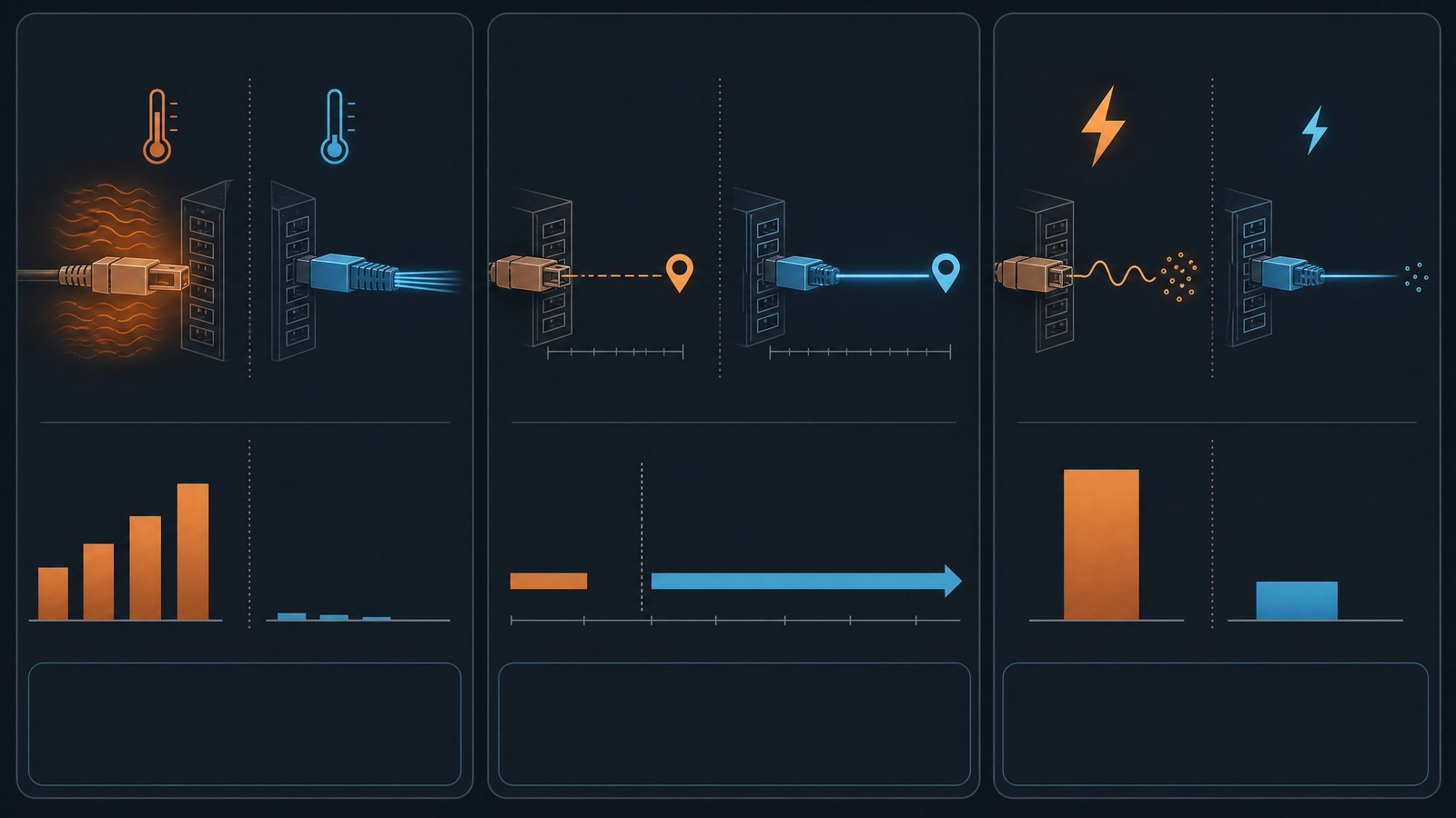
Copper's three limits: heat, distance, and energy per bit
And here is the figure that quantifies it
Arista reported in the second quarter that support for Linear Pluggable Optics cuts interconnect power consumption by roughly 60% versus traditional pluggable optics.
60% is not a technical improvement. It is a change in the budget.
In an AI data center, power is the binary constraint: there is a fixed number of megawatts the grid supplies, and the question is how much compute you can pack inside them. Every watt saved on interconnect is a watt available to feed another chip.
So photonics is not a nice-to-have for the industry. It is the way to increase what can be built inside the same power envelope.
The value chain, stage by stage
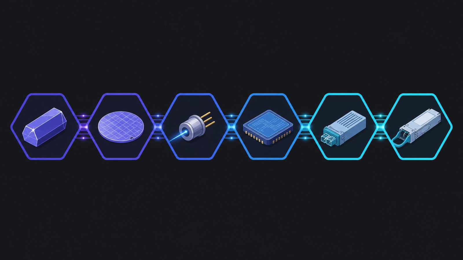
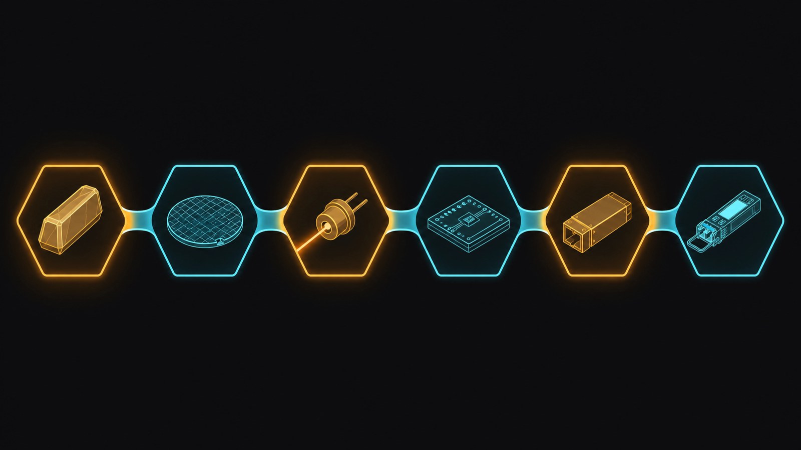
The six stages of the photonics chain: from raw crystal to transceiver
And here comes the part most coverage skips. "Photonics" is not one product but a chain of six stages, and entirely different companies sit at each.
Stage 1: raw material
Everything starts here, and so does the shortage.
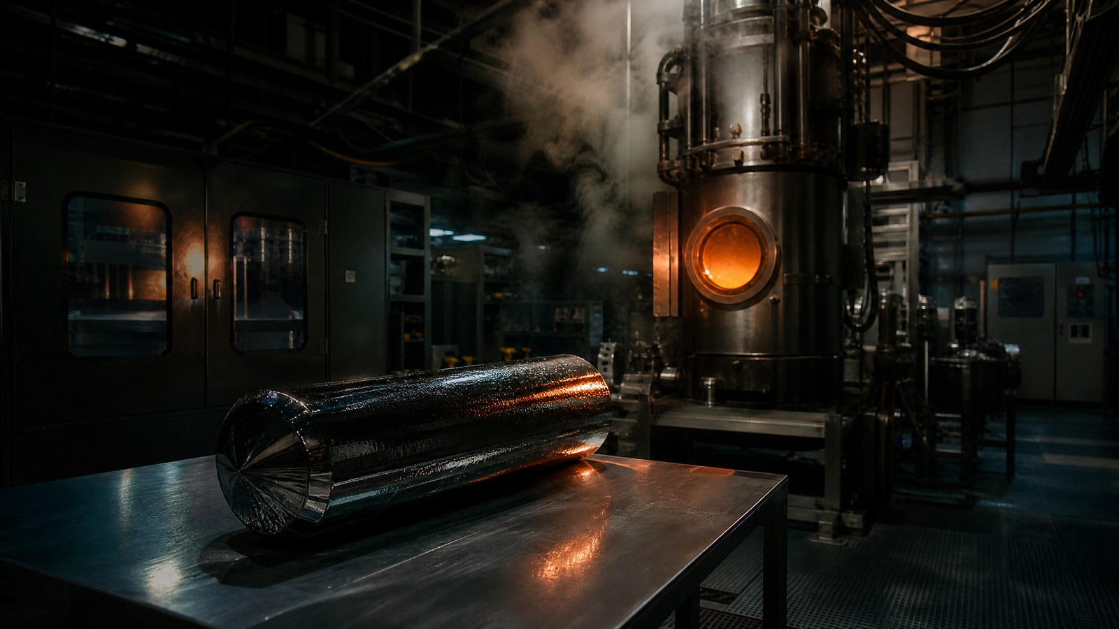
Stage 1: an indium phosphide crystal - where the laser begins
Silicon does not emit light. That is a basic physical fact, and it is the reason the whole chain exists. Producing a laser requires compound semiconductors - mainly indium phosphide (InP) and gallium arsenide (GaAs).
These are rarer, costlier and harder to grow than silicon. A quality InP crystal grows slowly, in smaller diameters, with higher scrap rates.
Who sits there: AXT, which makes InP and GaAs substrates, along with Soitec, IQE, IntelliEPI and Win Semiconductors across the substrate and epitaxy stages.
Stage 2: growing the layers
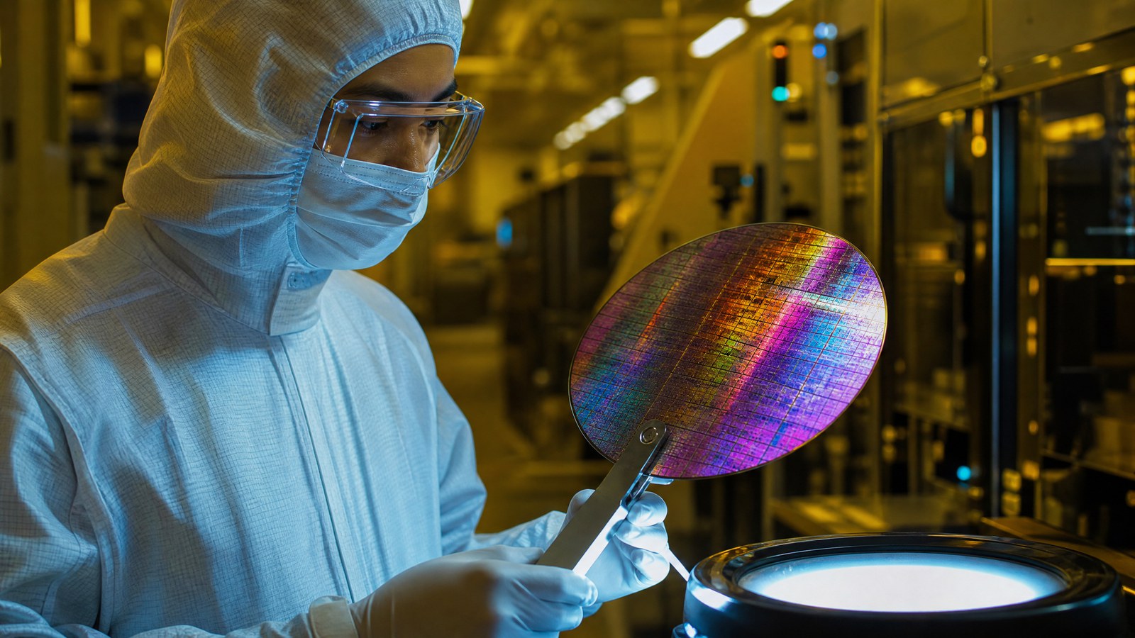
Stage 2: a wafer after epitaxy - layers a few atoms thick
On the substrate you must grow layers a few atoms thick - a process called epitaxy.
And the machine that does it is an MOCVD reactor. It costs millions of dollars, its lead time is measured in years, and very few manufacturers in the world build them.
Who sits there: Germany's Aixtron, and America's Veeco.
Stage 3: making the laser
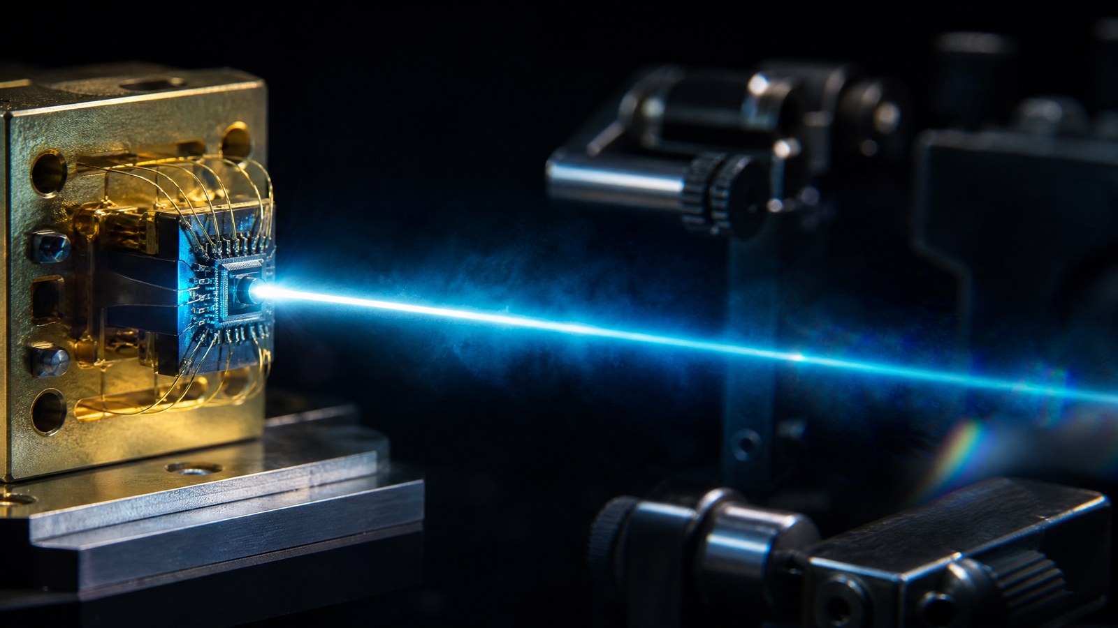
Stage 3: the laser diode - the component converting electricity into light
This is the active component - what converts an electrical signal into light.
Who sits there: Lumentum, Coherent, Taiwan's Landmark Optoelectronics, China's Yuanjie and Sweden's Sivers.
Stage 4: the foundry - silicon photonics
And here is the clever idea behind the whole field: rather than build the entire component from expensive materials, most of the optical circuit is made in ordinary silicon, on existing production lines, with only the InP laser attached to it.
That cuts cost dramatically and enables volume manufacturing.
Who sits there: Tower Semiconductor - which reported this week a $680 million annual run rate in silicon photonics against $180 million a year ago, and a plan to cross $1 billion in annual run rate in the fourth quarter.
Stage 5: packaging and assembly
The least discussed stage, and the narrowest.
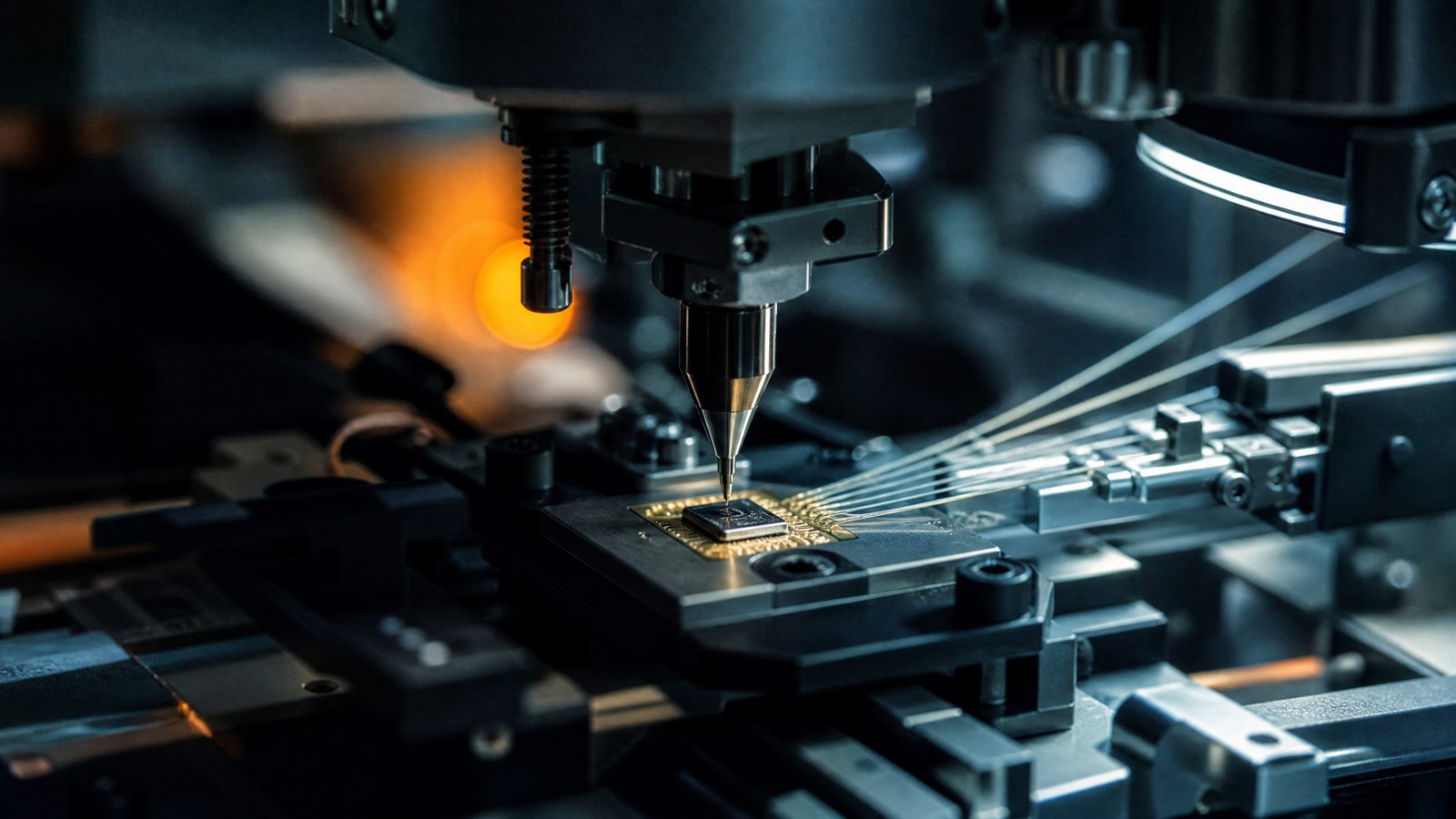
Stage 5: aligning fibre to chip - precision of a few microns
An optical fibre must be aligned to a chip within a few microns - and this must be done millions of times, cheaply, without breaking anything. It is work that resists automation.
Who sits there, at least on the test side: Aehr Test Systems, MPI and Chroma ATE.
Stage 6: the module and the system
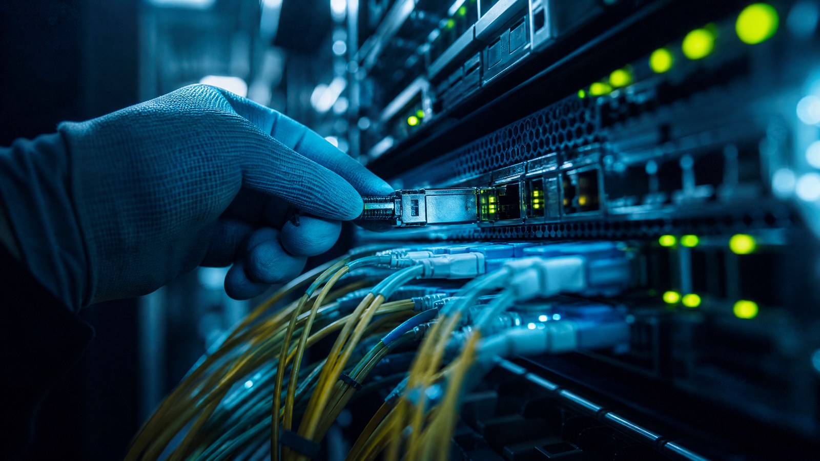
Stage 6: the optical transceiver - the product actually sold
The product actually sold - an optical transceiver that plugs into a switch.
Who sits there: Applied Optoelectronics, along with the large Chinese manufacturers Zhongji Innolight, Eoptolink and Suzhou TFC. And at the system end: Ciena, Arista, and Furukawa and Yangtze in fibre itself.
Where the real bottleneck sits
The three bottlenecks: raw material, epitaxy reactors and packaging
The shortage is not in silicon
And this is the point that matters most.
Stage 4 - silicon photonics - is actually the easiest stage to expand. It runs on existing foundry infrastructure, and there is available capacity in the world.
The shortage sits in three other places:
Stage 1 - raw material. Growing quality InP crystals takes time, and adding capacity takes years and heavy capital. You cannot double output because demand jumped.
Stage 2 - MOCVD reactors. A small number of makers, long lead times. Anyone who did not order a machine two years ago will not receive one this year.
Stage 5 - packaging. Micron precision at volume is an engineering problem that is not fully solved, and it is the stage where manufacturing yields break.
So: anyone looking at this field through the foundries is looking at the least constrained stage.
The fund that holds the whole chain
On 3 June 2026 a fund called the Tema Photonics & Optical ETF registered for listing on NYSE Arca, per the Form 8-A12B filed with the SEC.
It trades under the ticker LAZR.
And the ticker's story is worth pausing on
LAZR moved from a collapsed lidar company to a photonics fund
Until recently the ticker LAZR belonged to Luminar Technologies - a lidar company for autonomous vehicles.
And per its own SEC filings:
- Luminar and certain subsidiaries filed voluntary Chapter 11 petitions in the United States Bankruptcy Court for the Southern District of Texas, on 15 and 31 December 2025, jointly administered under Case No. 25-90807
- On 7 April 2026 it filed a Form 15-12G - deregistering its securities with the SEC
So the ticker was vacated through bankruptcy, and a photonics fund took it.
And that is a practical warning: anyone searching "LAZR" today and finding historical charts may be reading the share price of a collapsed lidar company while believing they are looking at a fund. Two entirely different assets, the same four letters.
What the fund holds
As of 5 August 2026, per the official holdings file - 28 positions, 100% of assets:
| Holding | Weight | Stage | Country |
|---|---|---|---|
| Lumentum | 14.77% | Lasers | US |
| AXT | 9.55% | InP substrates | US |
| Aixtron | 7.85% | MOCVD reactors | Germany |
| Anthropic SPV exposure | 7.30% | - | - |
| Cash | 6.24% | - | - |
| Applied Optoelectronics | 5.52% | Modules | US |
| Furukawa Electric | 4.71% | Fibre and cable | Japan |
| Aehr Test Systems | 4.45% | Test | US |
| Tower Semiconductor | 3.56% | Foundry | Israel |
| Landmark Optoelectronics | 3.12% | Lasers | Taiwan |
| Coherent | 2.76% | Lasers | US |
| Zhongji Innolight | 2.66% | Modules | China |
| Ciena | 2.66% | Systems | US |
| Eoptolink | 2.51% | Modules | China |
| Yangtze Optical Fibre | 2.37% | Fibre | China |
| Veeco | 2.24% | Equipment | US |
| Soitec | 2.23% | Substrates | France |
| IQE | 1.94% | Epitaxy | UK |
| Suzhou TFC Optical | 1.84% | Modules | China |
| Sivers Semiconductors | 1.68% | Lasers | Sweden |
| Yuanjie Semiconductor | 1.67% | Lasers | China |
| Himax | 1.47% | Optics | Cayman |
| IntelliEPI | 1.44% | Epitaxy | Cayman |
| Win Semiconductors | 1.37% | GaAs foundry | Taiwan |
| Semtech | 1.25% | Signal integrity | US |
| SiTime | 1.23% | Timing | US |
| MPI | 0.96% | Test | Taiwan |
| Chroma ATE | 0.64% | Test | Taiwan |
And reading that table teaches more than any description: the fund is built by stage in the chain, not by company size. Aixtron at 7.85% is a mid-sized equipment maker - but it is a link with no substitute.
Three things worth saying about this construction
1. The line that is hard to explain
7.30% of the fund sits in exposure to an Anthropic SPV.
Anthropic is not a photonics company. It is a private artificial intelligence lab that does not trade publicly. And an SPV is a dedicated vehicle holding exposure to a private company.
It is the fourth-largest holding in the fund - larger than Tower, than Coherent, than Ciena.
The logic is not hard to guess: buying photonics is really buying the demand of the AI labs. But it still means roughly 7% of a fund defined as photonics and optical sits in a private, illiquid asset outside the field.
Anyone buying the fund should know they are buying that too.
2. China is roughly 11% of the fund
Five Chinese companies - Zhongji Innolight, Eoptolink, Yangtze, Suzhou TFC and Yuanjie - together make up roughly 11% of assets.
And that is not incidental: China is the world's largest producer of optical transceivers. A fund genuinely describing the chain cannot skip it.
But it is also exposure to a non-commercial risk: export controls, tariffs and regulation from both directions. In an industry already at the centre of US-China technological competition, that is a risk worth pricing explicitly.
3. The fund is very new
A June 2026 listing means the fund has no meaningful performance history.
And in a new, niche fund, two further things deserve checking before buying: the size of assets under management, and the bid-ask spread - which in small funds holding positions in distant markets can be considerably wider than it appears.
Those figures change daily, so I have not quoted them here. They are on the fund page and in trading data, and are worth checking on the day one considers acting.
And not one fund - two, in the same week
And this is the sign hardest to ignore.
Alongside Tema, Roundhill ETF Trust also filed:
- On 3 August 2026 - a Form 8-A12B and summary prospectus for the Roundhill Photonics & Optics ETF
- On 5 August 2026 - the exchange certification for its ticker, LYTE
And it is an actively managed fund, unlike an index tracker. In the prospectus's words, it invests in the equity securities of companies "whose core technology involves generating, manipulating, detecting, or transmitting light".
The prospectus even takes the trouble to define the term: "Photonics refers to technologies that generate, detect, amplify, modulate, or process light at the device level - that is, technologies in which light is actively created, converted to or from electrical signals."
And why this is the important figure in this piece
Two dedicated photonics ETFs, from two different issuers, registering for listing two days apart.
Fund issuers do not launch a niche product because a subject is interesting. They launch it when they judge there is demand - and demand arrives after the numbers start showing up in reports, not before.
That is the difference between a thesis and the start of a cycle.
And for precision, the same Roundhill also filed an 8-A12B in those days for a different fund - the Roundhill Neocloud ETF - and Tema filed on 4 August for a Tema Power Semiconductor ETF on Cboe BZX. These are separate funds in adjacent fields, and confusing them is exactly the kind of mistake that is easy to make when an issuer launches several products in one week.
My Angle
A personal opinion of Ilan Abramov - not advice, not a recommendation
My thesis here is not about the technology. It is about timing.
Photonics was hype for years. A promise repeated at every conference, with handsome slides and no revenue. Anyone who bought it five years ago bought a story.
What changed is that it stopped being a promise and started appearing in reports. Tower went from a $180 million annual run rate in silicon photonics to $680 million within a year, and is targeting $1 billion in the fourth quarter. That is no longer a pilot - it is a revenue line doubling on itself.
So what I take from this piece is three things, in this order.
First, the value chain. Not "photonics" as one word, but six separate stages, each holding different companies with different economics. Anyone who does not take the chain apart is buying a random basket.
Second, the bottlenecks. And here is the surprise: the stage everyone looks at - silicon photonics - is the least constrained. It runs on existing foundries. The real bottlenecks are the InP crystal, the epitaxy reactors and the packaging - three places where capacity is built in years. And at a bottleneck, the margin moves to whoever sits on it.
And third, finding the winners. Not who talks about photonics, but who already shows it in the revenue line and the margin. The difference between the two will become clear over the next two years, and that is exactly the window I want to work in.
And what reinforces my read on timing is the external signal: two dedicated photonics ETFs registered for listing two days apart. Issuers do not launch a niche product before the numbers start arriving. They respond to demand rather than create it.
And what I keep in proportion: once a theme gets dedicated ETFs, it also gets money that does not check. That money lifts everything - the companies genuinely sitting on a bottleneck and the ones that merely sound like it. Which is why the real work starts now rather than ends here.
And you cannot discuss this field without discussing what the prices did. Photonics stocks rose by hundreds of percent from their 52-week lows to their spring peaks: Lightwave Logic about 1,380%, IQE about 1,190%, Lumentum about 1,060%, Applied Optoelectronics about 1,045%, Tower about 650%, and POET and Coherent about 390% each. That does not look like a market pricing a business. It looks like a market pricing a story.
And then they gave it back. From the May-June peaks to today: POET and Lightwave Logic down about 60%, Himax about 45%, Applied Optoelectronics about 42%, and IQE and Tower about a third. Anyone who entered at the peak absorbed half their position.
And here is the part that changed the picture for me. In the very week the reports landed, these stocks did not keep falling - they rose. Applied Optoelectronics gained about 17% that week, Fabrinet about 14.5%, Coherent about 14%, and POET about 10%. Not on an announcement and not on a conference, but on numbers.
And that is the difference between hype and a field starting to establish itself. Hype collapses and does not get back up, because there was nothing underneath it. What happened here is that the market stripped out the story premium, and then the reports showed there is a business underneath it. Those are two entirely different movements, and they are easy to confuse.
So where I stand today is two statements that live together. One: photonics is here to stay. It is no longer a promise; it is a revenue line in the filings of real manufacturers. And two: that does not mean the current valuation is justified. A field can be entirely real and still trade too expensively, and those two claims do not contradict each other.
And here I have to be precise about what I am not doing. I am not recommending any action - not in a stock, not in a fund, not in the sector - and I am not forecasting prices. I hold no licence to do that and I make no such claim. What I am saying is entirely conditional: if demand continues, if the deals intensify, and if these companies manage to convert the bottlenecks into margin, then there is room here for meaningful growth in value. And if not - the decline of recent months will turn out to be the beginning rather than the end. Both scenarios are open, and neither is certain.
Errors or inaccuracies are possible. Spotted something that looks wrong? Write to me and I will correct it.


