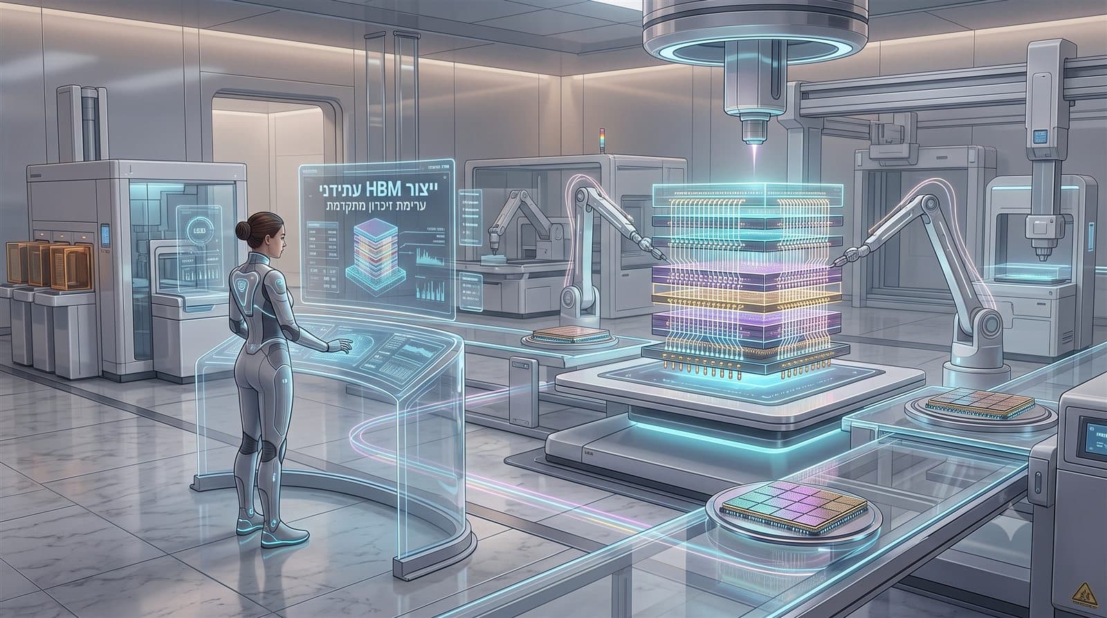
In the chip industry there is a rule of thumb: do not look at what companies announce, look at what they build. This week it was reported in the Korean industry that Samsung has begun building, at its Pyeongtaek campus (in the P5 complex), a mass-production line for Die-to-Wafer hybrid-bonding technology - and is running a procurement process for about 50 machines from Holland's BE Semiconductor (BESI), chosen as preferred supplier. Behind this technical sentence hides one of the more interesting stories of the AI era: the shift to the next generation of chip packaging, the new battlefield between the memory giants - and a value chain in which two Israeli companies sit in a particularly comfortable position.
Wait, What Is HBM Anyway - and Why Is Everyone Chasing It
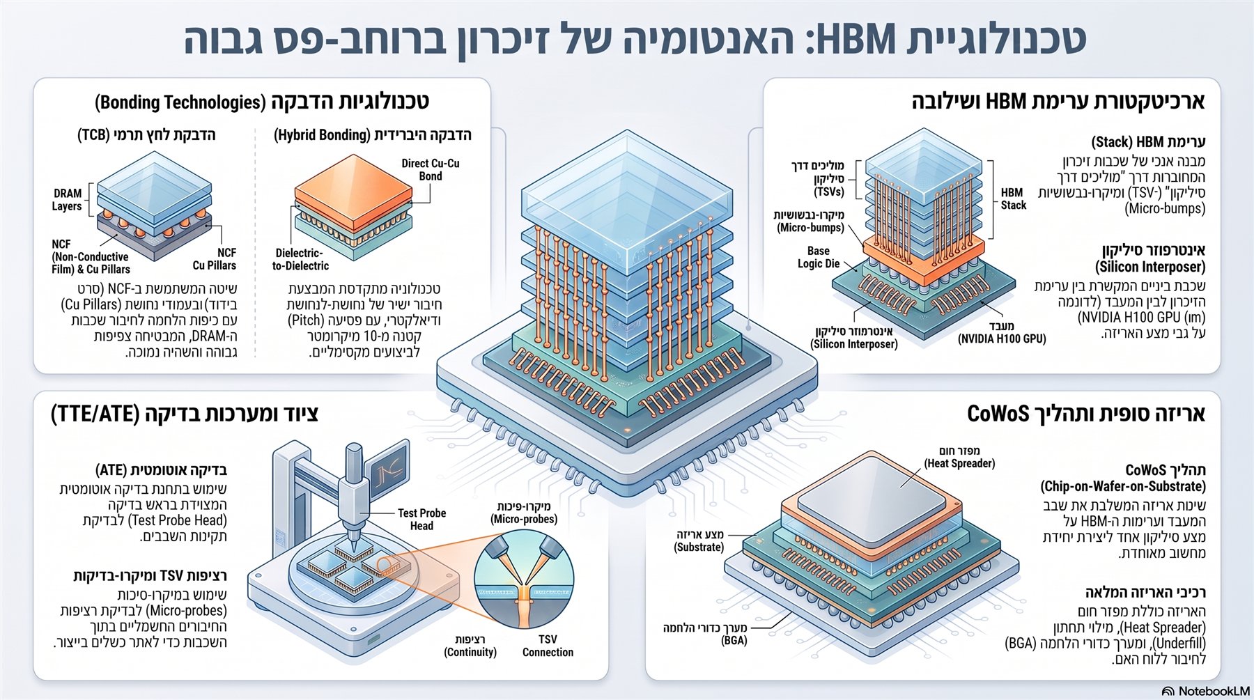
To understand the story you need two minutes of background. The most powerful AI processor in the world is worth very little if it has no fast enough way to read and write data - and ordinary memory simply cannot keep up. The industry's solution is called HBM (High Bandwidth Memory): instead of spreading memory chips across a board, they are stacked vertically - 8, 12 and soon 16 stories of DRAM chips one on top of another, connected by vertical channels - and the tower is placed right next to the processor. The result: enormous bandwidth millimeters from the GPU. Every advanced NVIDIA or AMD AI accelerator is wrapped today in HBM stacks, and demand is so strong that memory makers sell capacity years ahead. This is also the industry's big business fight: SK Hynix leads this market, and Samsung - the giant used to leading in every memory field - is fighting to win back the crown.
And What Is Hybrid Bonding - and Why Is It the Next Step
Here enters the technology at the heart of the Pyeongtaek investment. Today, the DRAM stories in an HBM tower are connected to each other via micro-bumps - tiny metal balls soldered under pressure and heat (a method known as TC Bonding). It works, but it has a cost: each layer of balls adds height, lengthens the electrical path and generates heat.
Hybrid Copper Bonding dispenses with the balls entirely: the copper and insulating surfaces of two chips are pressed and bonded directly to each other, atom to atom. The practical meaning: a lower, denser tower, shorter electrical paths, lower power and significantly better heat dissipation - Samsung itself published figures quantifying a considerable cooling advantage. The taller the towers (16 stories and up), the more these advantages turn from "nice" to "essential": at such heights, the old method approaches the edge of its capability.
The Detail That Changes the Picture: Real Demand Is Far From 2026
And now to the nuance that makes the story truly interesting. Despite the construction at Pyeongtaek, hybrid bonding will not enter mass production of the coming HBM4 generation: the JEDEC standards body eased the package-thickness limits, allowing makers to continue with the existing method for another generation, and per reports Samsung and SK Hynix pushed mass adoption to 16-story HBM4E - and in the full scenario to HBM5. Inside Samsung, per those reports, large-scale production in the technology is estimated to mature only around 2030, and an industry source tied the timing to NVIDIA's next-generation accelerator (codenamed Feynman), expected around 2029.
So why build a mass line already now, and install machines this year? For three reasons, all strategic:
- The learning curve. Hybrid bonding is significantly harder than the existing method - exactly why Samsung is setting up an early line. Whoever masters the process first will reach economical yields first, and that is the difference between profit and loss in memory.
- Custom memory (cHBM). The next generation of the market is HBM in which the base
layer is not a generic helper chip but a logic chip with the customer's intellectual
property - a kind of built-in helper computer at the bottom of the memory tower. Samsung
is planning an architecture in which the DRAM layers are stacked directly on the logic chip
- and that is almost impossible without hybrid bonding. Here Samsung is trying to build an advantage that would leapfrog the rival's lead.
- Not just memory. Samsung's Foundry division recently unveiled a hybrid-bonding-based 3D packaging solution (named 3D Cube-H) for AI and supercomputing chips - meaning that same Pyeongtaek line serves a vision broader than HBM alone.
The Equipment War: BESI vs. the Korean Revolt
And here comes the sharpest business part of the story. Holland's BESI (EURONEXT: BESI) is the global market leader in hybrid bonding - its machines serve TSMC and Micron, and it has a strategic partnership with Applied Materials (NASDAQ: AMAT) on an integrated system. Samsung chose it as preferred supplier for the new line, and per reports a procurement of about 50 machines is underway - which at the reported price of about $4.3 million per machine implies an order potential of more than $200 million.
But the deal is being delayed, and the reasons are instructive: Samsung demands adjustments to the machine architecture, and BESI - which sells to the entire industry - is in no rush to build a unique version for a single customer. And above all: BESI's machines are about twice as expensive as rivals'. That price premium is exactly the opening through which the "Korean revolt" enters: SEMES, Samsung's own equipment subsidiary, completed development of its own D2W machine and delivered a unit for qualification tests - and aspires to win two lines at Pyeongtaek; and Hanwha Semitech completed a second generation of its own machine and already delivered an evaluation unit to SK Hynix. The pattern is familiar from the history of the Korean chip industry: from dependence on an expensive Western supplier, to local development, and from there to erosion of the premium. An investor in BESI must hold both thoughts at once: real technological leadership today, and real localization risk tomorrow.
The chart shows BESI's U.S. ADR (ticker BESIY), which tracks the stock traded in Amsterdam.
The Israeli Angle: Who Wins in Every Scenario
And now to the part that interests us most. In the question "which bonding machine will win" there is risk - but there is a layer in the value chain that wins regardless of the answer: testing and metrology. The more advanced the packaging, the smaller the margin for error: copper surfaces bonded atom-to-atom demand flatness and cleanliness at unprecedented levels, and a 16-story tower where each story underwent dozens of processing steps is a nightmare of failure points. The result: every next-generation HBM stack passes through more testing and measurement stations than ever - and whoever sells these stations profits whether hybrid arrives in 2027, in 2029, or even if TC survives another generation.
Here sit two Israeli companies. Camtek (NASDAQ: CAMT) from Migdal HaEmek, whose inspection platform is designed exactly for this world - HBM, chiplets and hybrid bonding, with the ability to handle hundreds of millions of connection points on a wafer - presents the proof in numbers: an order of about $25 million from a leading chip maker (adding to $45 million cumulative from the same customer for 2026 delivery), a multi-system order of about $31 million from a leading OSAT, and per company management - orders and forecasts from two HBM makers with expected revenue of over $260 million for 2026-2027. Nova (NASDAQ: NVMI) from Rehovot completes the picture on the metrology side - measuring the layers and structures during the manufacturing process itself - a field that becomes critical as packaging turns three-dimensional. America's KLA and Onto also operate in the arena, but the Israeli starting point here is particularly strong relative to the size of the companies.
What Could Go Wrong
As usual, the other side of the coin. The timing has already been pushed once - from adoption in HBM4 to HBM4E - and there is no guarantee it will not be pushed again; whoever prices in hybrid revenue in 2027 may be waiting. BESI's negotiation with Samsung could end in a smaller-than- expected share - or in a Korean win - and the 2x price premium is a real weak point. Samsung itself has to prove execution: in the previous HBM generation it lost the lead, and the bet on cHBM is an attempt to leapfrog - not a done deal. And finally, valuation: Camtek and its peers already trade at multiples that price in a substantial part of the growth, and the high backlog is a double-edged sword if the memory makers' investment season moderates. As always - a correct thesis and an expensive stock can live in the very same security.
The Bottom Line
The Pyeongtaek P5 story is another example of the pattern we have been tracking all week, from power scarcity to earnings season: the infrastructure of the next revolution is built years before it shows up in the revenue line. Samsung is installing this year machines for production that will mature only toward the end of the decade, and is willing to pay in advance for the learning curve - because in an industry where leadership changes once a generation, whoever is late to the next packaging technology is late for the whole decade. For the investor, the opportunity is not in guessing who will win the machine war - but in identifying the links that benefit from the shift itself. And this time, two of them speak Hebrew.
Sources: Korean and international industry reports (including The Elec and TrendForce), companies' public announcements and statements (Samsung, BESI, Camtek), and public market data - current as of the time of writing. Procurement details not yet finalized are based on reports and may change. The charts are shown in real time via TradingView.


